Assembly-Related Productization Activities
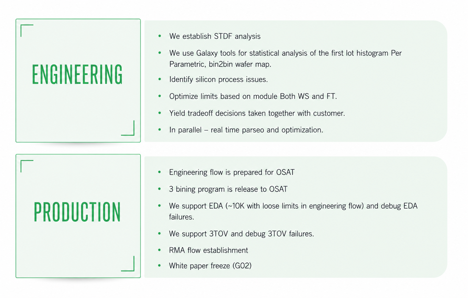
Prior to selecting an assembly and test vendor, our engineering and production teams evaluate parameters such as the technical and thermal characteristics of the package; existing and forecasted applications of the chip; estimated production volumes; vendor's capacity, location and overall profile, and availability for future test platforms.
Once the package type and vendor are selected, we will design the package bonding diagram and substrate according to the specification. We will perform the package simulations. Additionally, we will coordinate the timely delivery of the tooling, the prototype run, and a smooth transfer of the test program to production.
AAS has the capability to design packages of any complexity:
- BGA, Flip Chip BGA, LGA, Cu Pillar, WLCSP, QFP, a-QFP, Glass Topped BGA, etc
- AAS has experience in 2.5D packaging, Interposer (CoWos), and SiP design and manufacturing.
- AAS can complement the package with dies and passive components provided by Avnet.
Test-Related Productization Activities
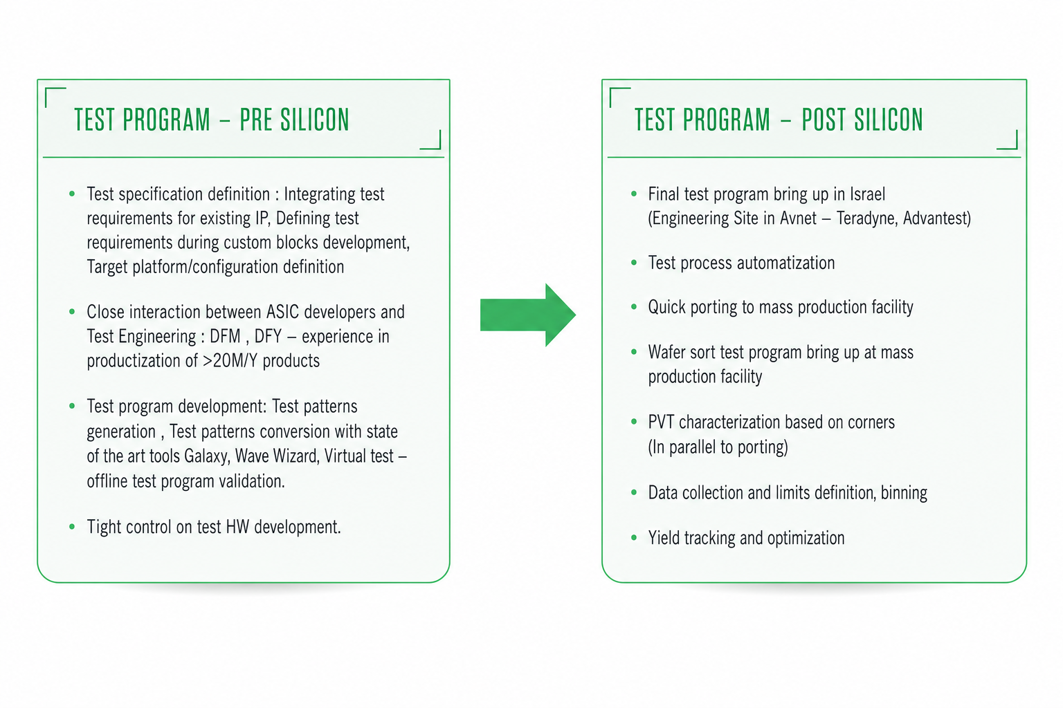
Our engineering team has extensive knowledge of all leading test platforms, such as Teradyne and Advantest, and is capable of selecting the best platform to meet our customers' requirements.
Our on-site equipment includes Teradyne and Advantest testers and a three temperatures handler, all fully compatible with leading OSAT mass production configurations. The testers are used for AAS test programs development and are also available for rental.
We also have a Synax S4 three-temperatures handler designed for low-to-medium production volumes.
We design test hardware, such as tester loadboards, sockets, and probe cards for wafer sort. We manage test program development, debugging, and production integration. Our objective is to ensure that the test program is robust enough to detect any possible manufacturing flaws.
AAS's manufacturing team coordinates test program transfer to the selected foundry for the wafer sort and to the chosen assembly and/or test house for the final test. Our ultimate goal is to create a solid, stable and aligned test program at the fab and test house, ensuring high coverage for both wafer probing and final testing.